- 您现在的位置:买卖IC网 > Sheet目录3854 > PIC18F4450-I/PT (Microchip Technology)IC PIC MCU FLASH 8KX16 44TQFP
147
XMEGA A [MANUAL]
8077I–AVR–11/2012
Bits 3:2 – Reserved
These bits are unused and reserved for future use. For compatibility with future devices, always write these bits to zero
when this register is written.
Bit 1:0 – CLKOUT[1:0]: Clock Output Port
These bits decide which port the peripheral clock will be output to. Pin 7 on the selected port is the default used. The
CLKOUT setting will override the EVOUT setting. Thus, if both are enabled on the same port pin, the peripheral clock will
be visible. The port pin must be configured as output for the clock to be available on the pin.
Table 13-9 on page 147 shows the possible configurations.
13.15 Register Descriptions – Virtual Port
13.15.1 DIR – Data Direction register
Bit 7:0 – DIR[7:0]: Data Direction
This register sets the data direction for the individual pins in the port mapped by VPCTRLA, virtual port-map control
register A or VPCTRLB, virtual port-map control register B. When a port is mapped as virtual, accessing this register is
identical to accessing the actual DIR register for the port.
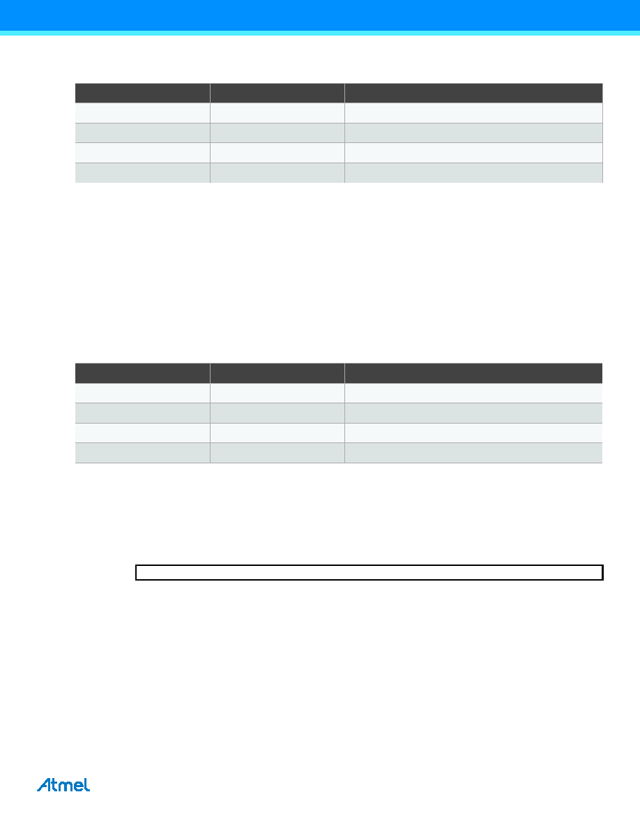
Table 13-8. Event output pin selection.
EVOUT[1:0]
Group configuration
Description
00
OFF
Event output disabled
01
PC
Event channel 0 output on PORTC
10
PD
Event channel 0 output on PORTD
11
PE
Event channel 0 output on PORTE
Table 13-9. Clock output port configurations.
CLKOUT[1:0]
Group configuration
Description
00
OFF
Clock output disabled
01
PC
Clock output on PORTC
10
PD
Clock output on PORTD
11
PE
Clock output on PORTE
Bit
7
6
543
210
+0x00
DIR[7:0]
Read/Write
R/W
Initial Value
0
发布紧急采购,3分钟左右您将得到回复。
相关PDF资料
21FMN-BMTTR-A-TB
CONN FMN HSNG 21POS STAG REV SMD
PIC16LF87-I/ML
IC MCU FLASH 4KX14 EEPROM 28QFN
PIC24HJ32GP204-I/PT
IC PIC MCU FLASH 32K 44TQFP
20FMN-BMTTR-A-TB
CONN FMN HSNG 20POS STAG REV SMD
PIC16F88-I/SS
IC MCU FLASH 4KX14 EEPROM 20SSOP
18FMN-BMTTR-A-TB
CONN FMN HSNG 18POS STAG REV SMD
17FMN-BMTTR-A-TB
CONN FMN HSNG 17POS STAG REV SMD
PIC18LF46J11-I/ML
IC PIC MCU FLASH 64K 2V 44-QFN
相关代理商/技术参数
PIC18F4450T-I/ML
功能描述:8位微控制器 -MCU 16KB FL 768 RAM 34 I/O FS-USB 2.0 RoHS:否 制造商:Silicon Labs 核心:8051 处理器系列:C8051F39x 数据总线宽度:8 bit 最大时钟频率:50 MHz 程序存储器大小:16 KB 数据 RAM 大小:1 KB 片上 ADC:Yes 工作电源电压:1.8 V to 3.6 V 工作温度范围:- 40 C to + 105 C 封装 / 箱体:QFN-20 安装风格:SMD/SMT
PIC18F4450T-I/PT
功能描述:8位微控制器 -MCU 16KB FL 768 RAM 34 I/O FS-USB 2.0 RoHS:否 制造商:Silicon Labs 核心:8051 处理器系列:C8051F39x 数据总线宽度:8 bit 最大时钟频率:50 MHz 程序存储器大小:16 KB 数据 RAM 大小:1 KB 片上 ADC:Yes 工作电源电压:1.8 V to 3.6 V 工作温度范围:- 40 C to + 105 C 封装 / 箱体:QFN-20 安装风格:SMD/SMT
PIC18F4455-BL
制造商:POWERLITE SYSTEMS 功能描述:PIC18F445 W/ BOOTLOADER FOR FLASHLAB 制造商:POWERLITE SYSTEMS 功能描述:PIC18F445 W/ BOOTLOADER, FOR FLASHLAB 制造商:POWERLITE SYSTEMS 功能描述:PIC18F445 W/ BOOTLOADER, FOR FLASHLAB; Silicon Manufacturer:Powerlite Systems; Core Architecture:PIC; Kit Contents:Board; Features:Bootloader Programming, RS232 Connector for Boot-Loading and Serial Comms ;RoHS Compliant: Yes
PIC18F4455-I/ML
功能描述:8位微控制器 -MCU 24kBF 2048RM FSUSB2 RoHS:否 制造商:Silicon Labs 核心:8051 处理器系列:C8051F39x 数据总线宽度:8 bit 最大时钟频率:50 MHz 程序存储器大小:16 KB 数据 RAM 大小:1 KB 片上 ADC:Yes 工作电源电压:1.8 V to 3.6 V 工作温度范围:- 40 C to + 105 C 封装 / 箱体:QFN-20 安装风格:SMD/SMT
PIC18F4455-I/P
功能描述:8位微控制器 -MCU 24kBF 2048RM FSUSB2 RoHS:否 制造商:Silicon Labs 核心:8051 处理器系列:C8051F39x 数据总线宽度:8 bit 最大时钟频率:50 MHz 程序存储器大小:16 KB 数据 RAM 大小:1 KB 片上 ADC:Yes 工作电源电压:1.8 V to 3.6 V 工作温度范围:- 40 C to + 105 C 封装 / 箱体:QFN-20 安装风格:SMD/SMT
PIC18F4455-I/PT
功能描述:8位微控制器 -MCU 24kBF 2048RM FSUSB2 RoHS:否 制造商:Silicon Labs 核心:8051 处理器系列:C8051F39x 数据总线宽度:8 bit 最大时钟频率:50 MHz 程序存储器大小:16 KB 数据 RAM 大小:1 KB 片上 ADC:Yes 工作电源电压:1.8 V to 3.6 V 工作温度范围:- 40 C to + 105 C 封装 / 箱体:QFN-20 安装风格:SMD/SMT
PIC18F4455T-I/ML
功能描述:8位微控制器 -MCU 24kBF 2048RM FSUSB2 RoHS:否 制造商:Silicon Labs 核心:8051 处理器系列:C8051F39x 数据总线宽度:8 bit 最大时钟频率:50 MHz 程序存储器大小:16 KB 数据 RAM 大小:1 KB 片上 ADC:Yes 工作电源电压:1.8 V to 3.6 V 工作温度范围:- 40 C to + 105 C 封装 / 箱体:QFN-20 安装风格:SMD/SMT
PIC18F4455T-I/PT
功能描述:8位微控制器 -MCU 24kBF 2048RM FSUSB2 RoHS:否 制造商:Silicon Labs 核心:8051 处理器系列:C8051F39x 数据总线宽度:8 bit 最大时钟频率:50 MHz 程序存储器大小:16 KB 数据 RAM 大小:1 KB 片上 ADC:Yes 工作电源电压:1.8 V to 3.6 V 工作温度范围:- 40 C to + 105 C 封装 / 箱体:QFN-20 安装风格:SMD/SMT